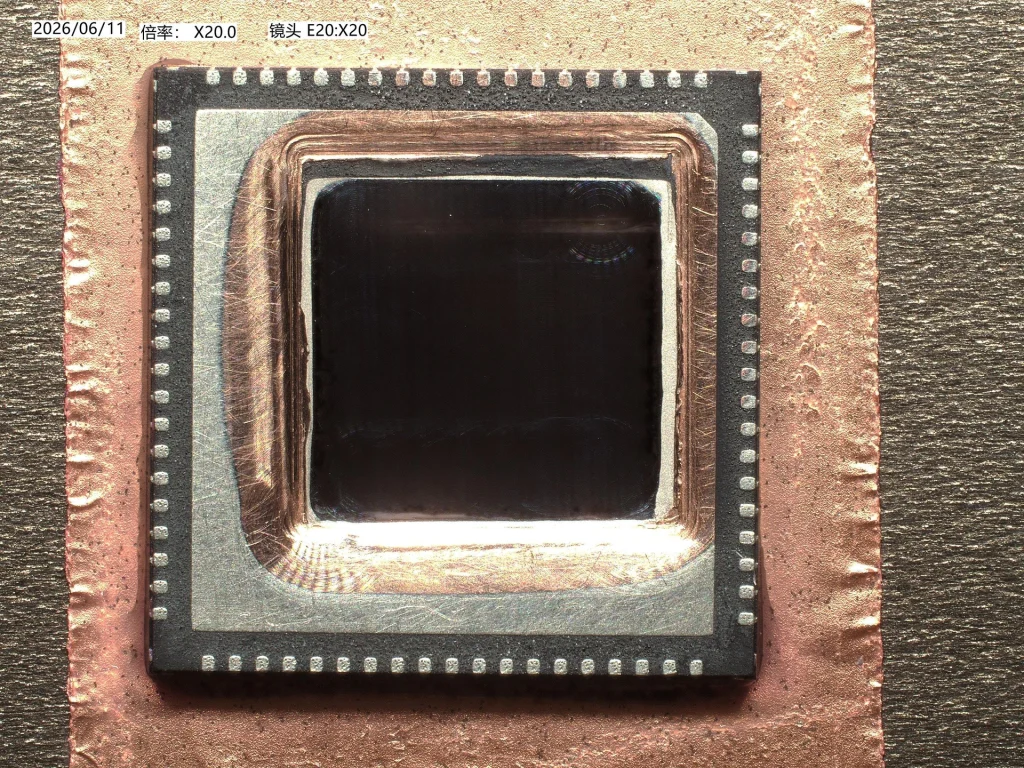
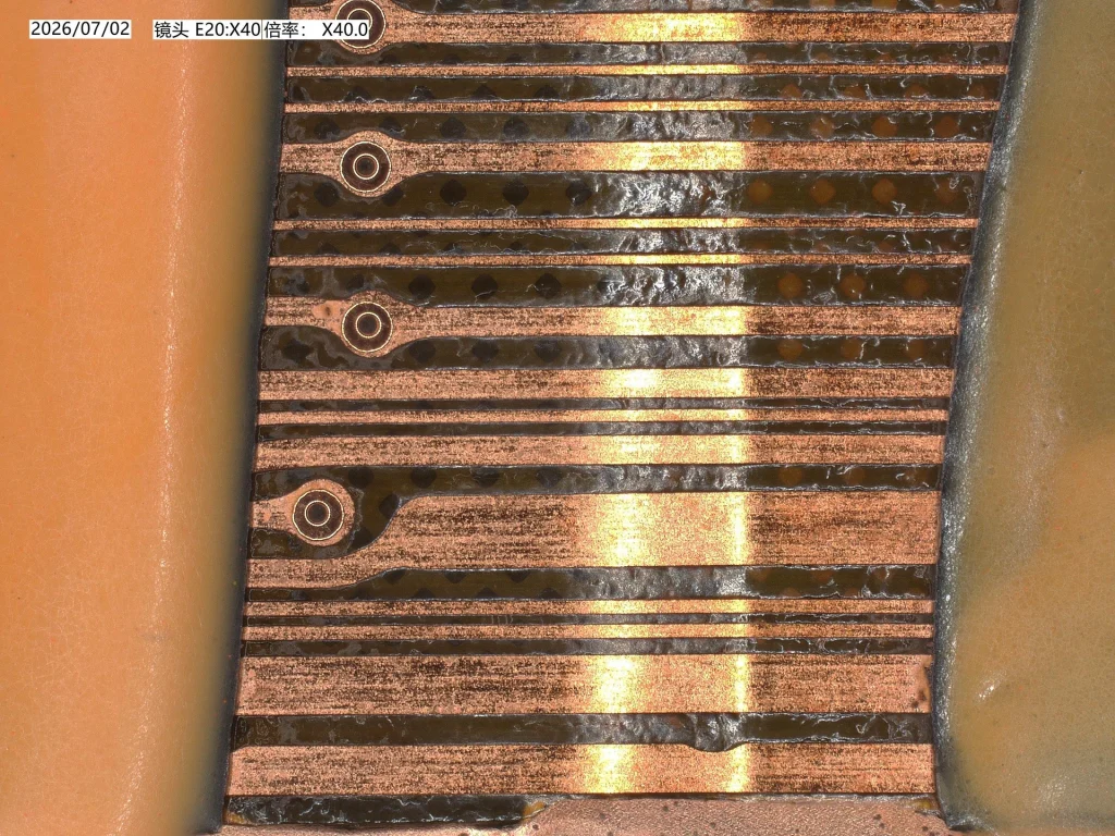
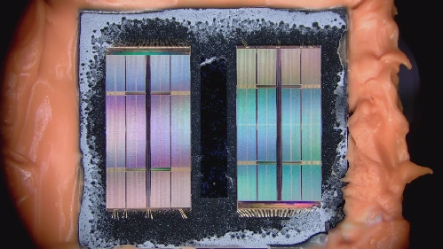
iMech Pro application images illustrate chip backside thinning, with a process path combining height measurement, leveling, visual positioning and suitable remaining-silicon-thickness metrology.
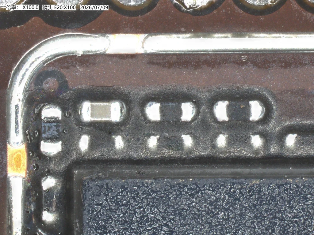
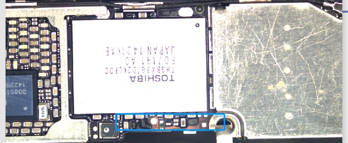
Local motherboard images illustrate Encap adhesive and PCB solder-mask removal, with inspection requirements for exposed regions, neighboring components and metal surfaces.
The source records approximately 4 hours for an A13-marked sample and approximately 3 hours for another package, both using plasma only without laser preprocessing.
Combine small-area opening with peelable protective material to limit the processing region and support review of the target chip and neighboring structures.
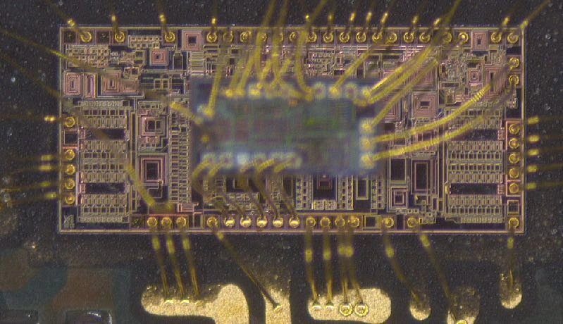
Explore the challenges of stacked-die and memory-package decapsulation, two real application examples, and a combined iMech Pro and MIP route for subsequent die delayering.
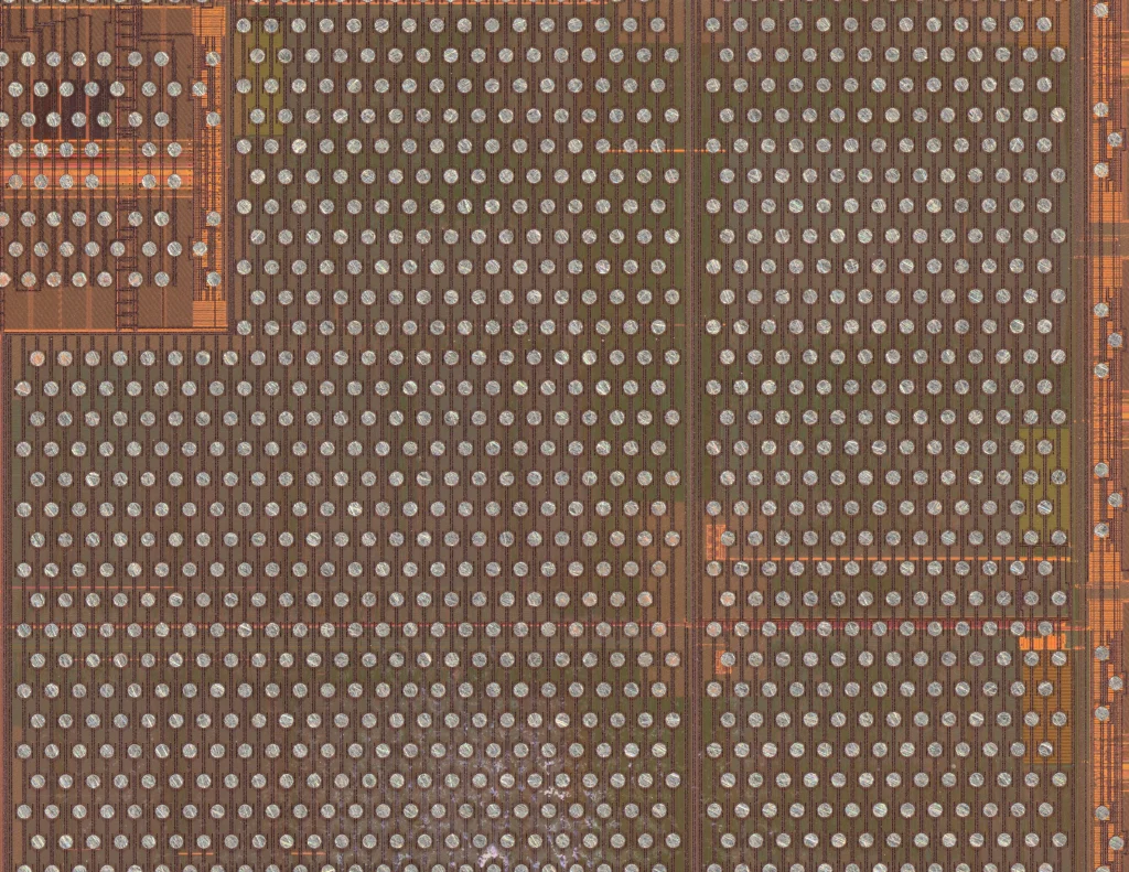
A 3D package decapsulation case for semiconductor failure analysis: MIP plasma underfill removal after customer grinding, μbump inspection, and a proposed local workflow combining iMech Pro with iPlasma MIP.
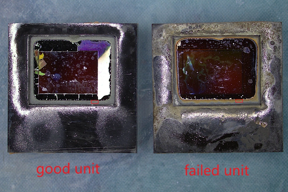
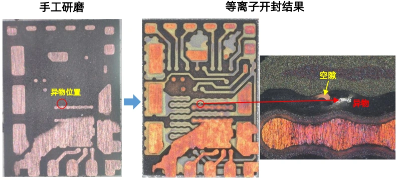
Compare broad manual grinding with iMech Pro local opening for a published flip-chip micro-short case. Targeted access and MIP residue removal can help retain electrical connections for post-decapsulation retesting.