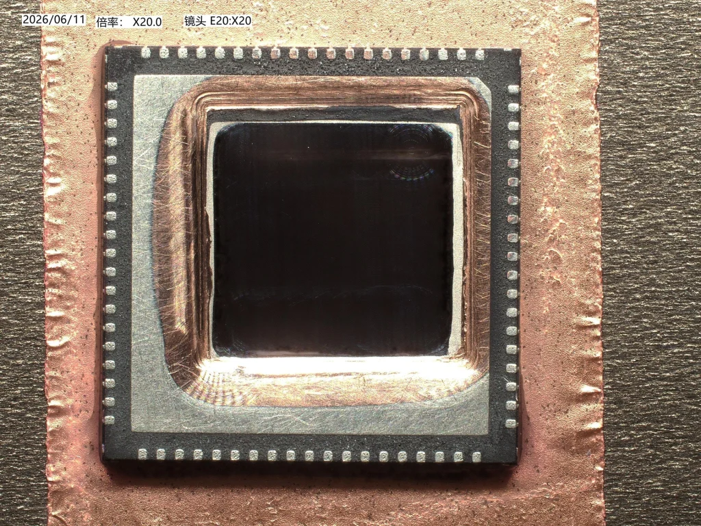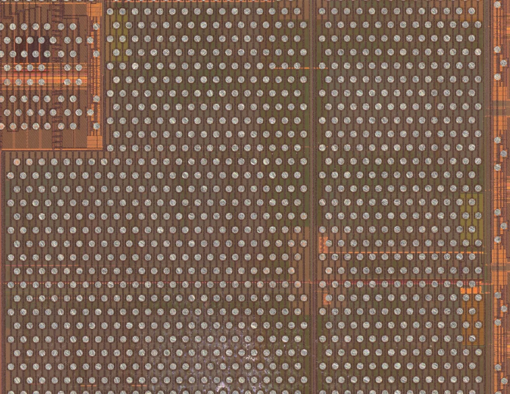
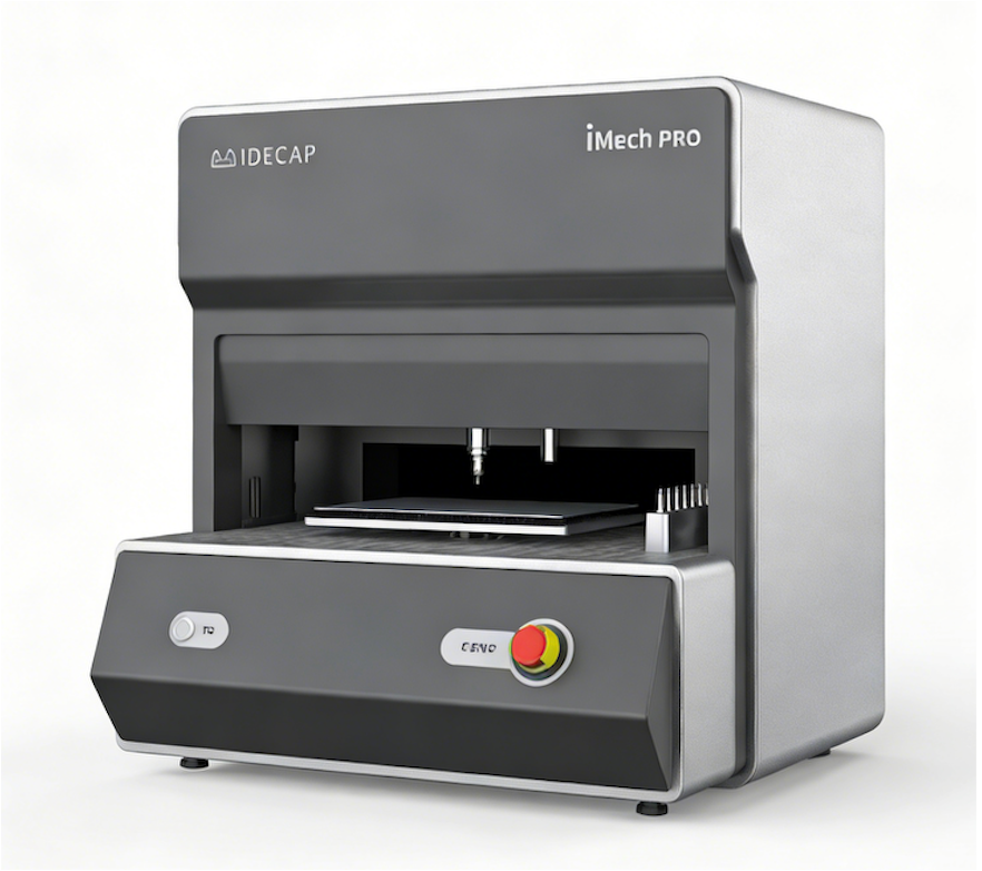
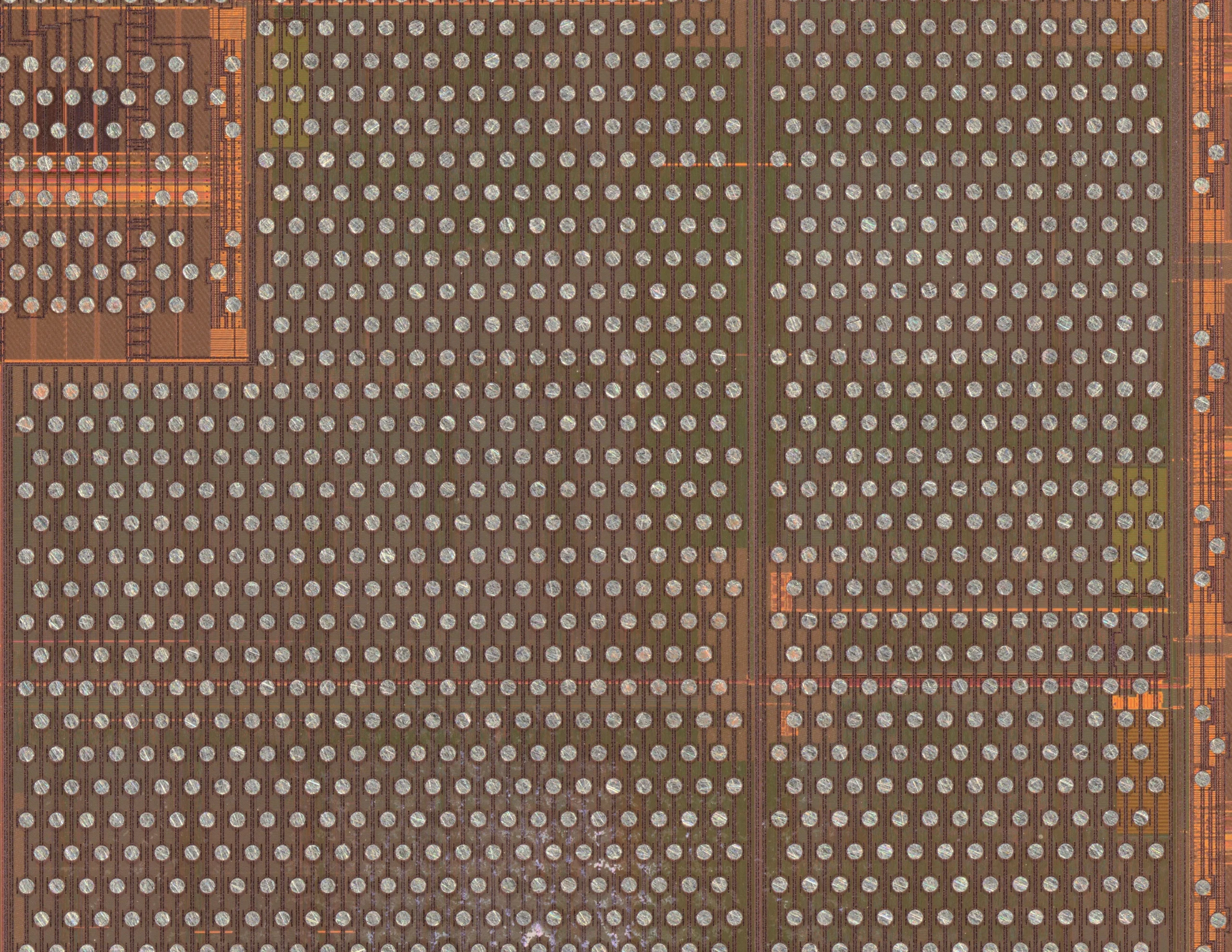
For chip backside thinning, local mechanical decapsulation and preparation trials on complex material structures.
Multiple preparation methods
Choose milling, grinding or polishing according to the material and analysis objective, connecting rough processing with finishing.
Control position and thickness
Use leveling, position control and suitable thickness metrology to establish a layered removal path.
Evaluate additional applications
Local removal of adhesive-covered components can be evaluated; retention of original solder requires sample-specific validation.
Technical overview
| Item | Published specification / application information |
|---|---|
| Processing area | 300 × 200 mm |
| Z-axis resolution | 20 nm |
| Nominal overall Z-axis accuracy | Better than 1 μm |
| Maximum spindle speed | 60,000 rpm |
Resolution is not actual machining accuracy. RST measures remaining silicon thickness and must not be used to promise residual solder or adhesive thickness. Each application requires independent validation.
Suggested process sequence
- Position and level
- Remove material in layers
- Verify thickness and surface condition
Information for sample evaluation
- Package and material type, target structures and areas to preserve
- Sample dimensions, structural images, failure state and downstream analysis method
- Agreed methods for surface, structure or thickness verification
Six capabilities across positioning, processing and review
Combine modules around the sample and application objective. These capabilities follow the iMech Pro technical material; modules, measurement ranges and acceptance criteria depend on technical confirmation and the delivered configuration.
01 Precision milling & polishing
Supports 2D / 3D contour processing and target-area thinning. The source specifies 20 nm axis resolution and nominal overall accuracy better than 1 μm. Actual workpiece results require separate validation.
02 Chromatic confocal height measurement
Capture surface topography, local height and warpage as inputs for leveling, compensation and post-process review.
03 Optical vision positioning
Locate and observe the target area, selecting a suitable field of view and magnification for the sample features.
04 IR + visible-spectrum RST
Measures remaining silicon thickness under applicable conditions. It does not directly establish residual solder or adhesive thickness.
05 Dual R-axis leveling
Combine Z and dual R-axis adjustments to set the local processing orientation and assess the effects of tilt and warpage.
06 Force control
Monitor and control contact load to help manage overcut, edge chipping and surface consistency.
Application images
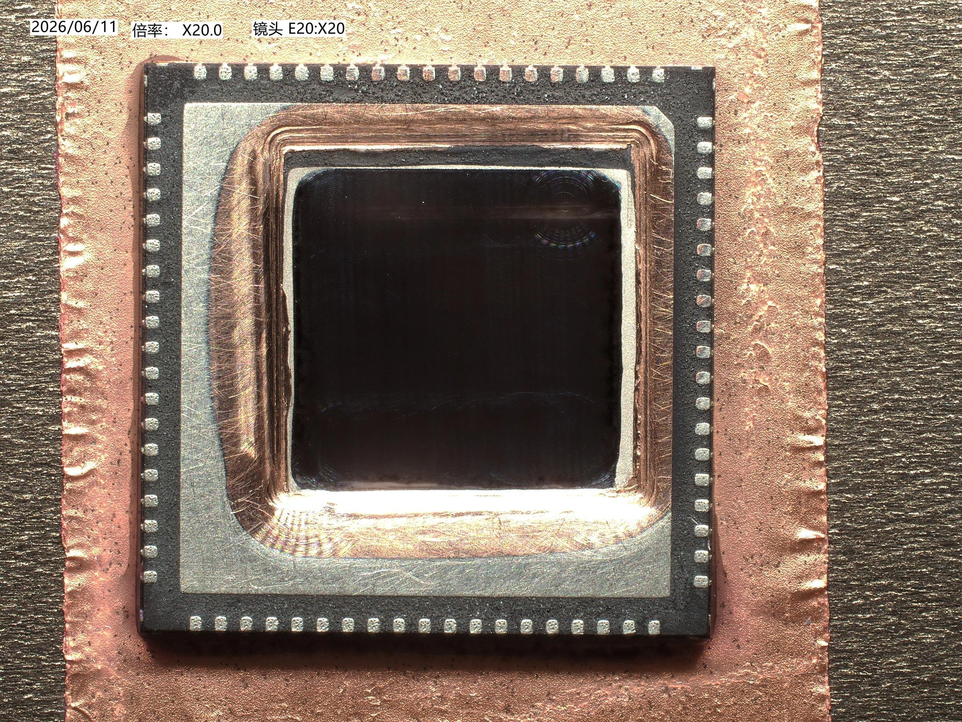
Explore mechanical thinning → Explore 3D package delayering →