
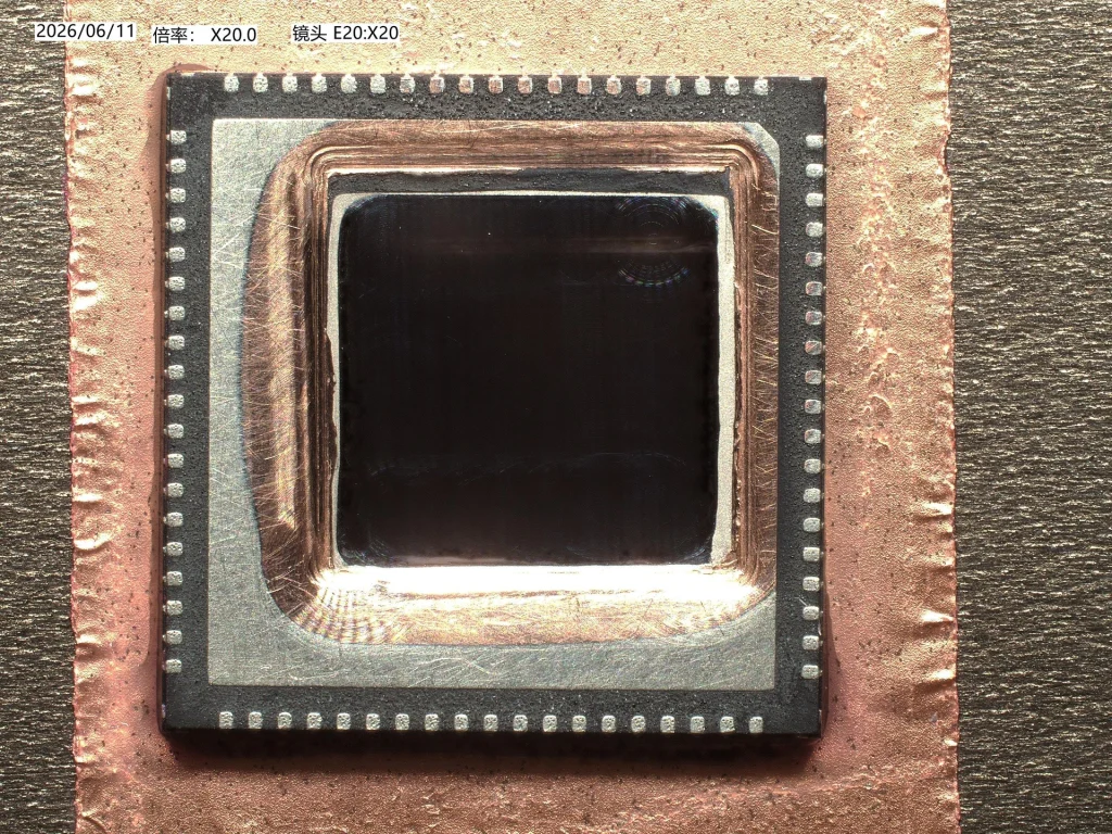
Sample and analysis objective
Mechanical thinning must achieve the thickness and surface condition needed for downstream analysis while controlling local tilt, contact load and edge effects.
| Item | Case information |
|---|---|
| Application direction | Chip backside and local silicon thinning |
| Process control | Height measurement, leveling, positioning and layered removal |
| Thickness verification | RST measures remaining silicon thickness; confirm suitability for the actual material and configuration |
Processing record
The source labels this a wafer-thinning application example. The image shows a chip region within a package and does not establish full-wafer processing dimensions or thickness-uniformity performance.
Actual sample images
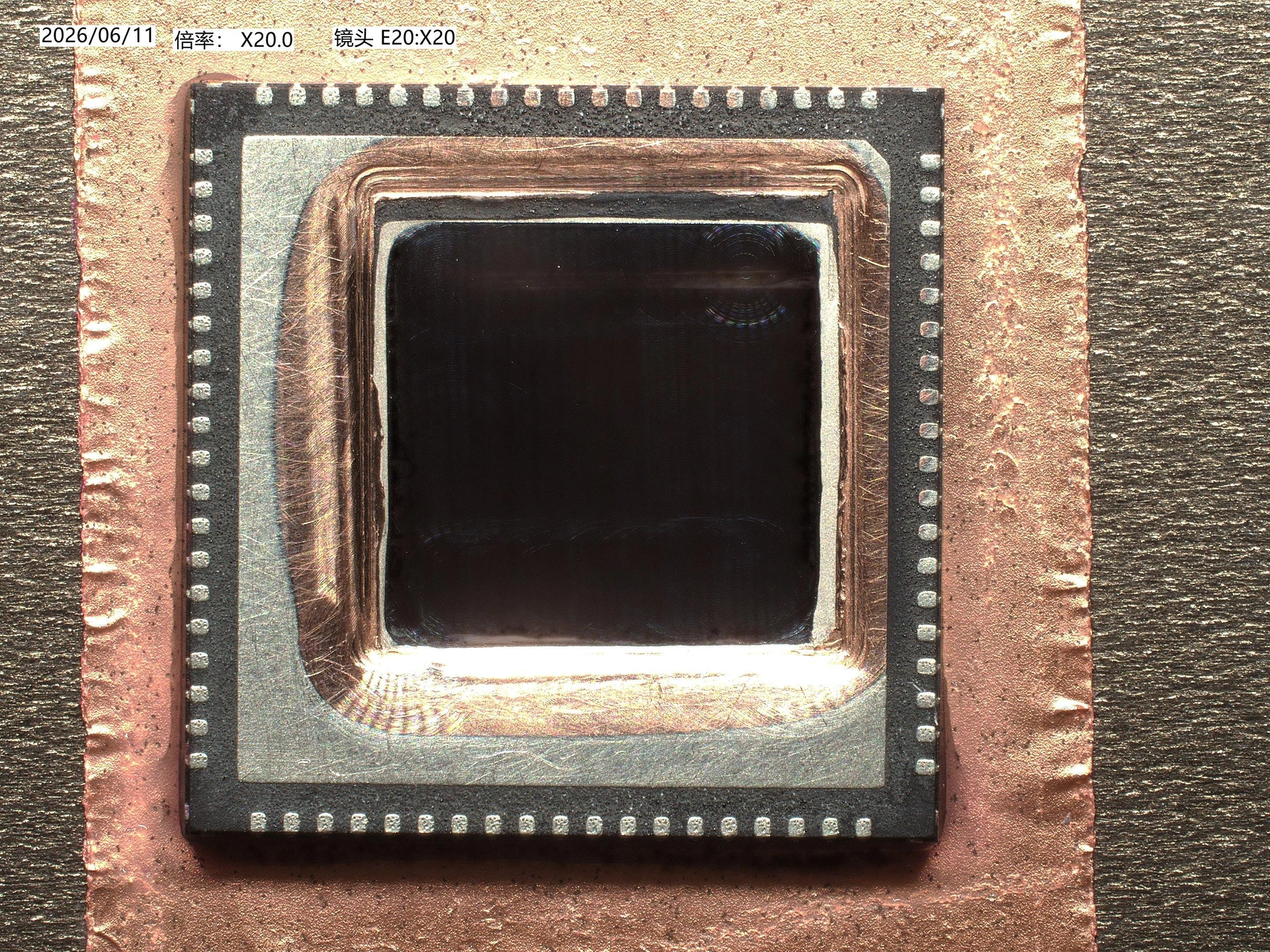
Result review priorities
- Define initial thickness, target thickness and permissible local variation.
- Evaluate axis resolution, nominal equipment accuracy and actual sample results separately.
- In addition to thickness, inspect surfaces, edges, flatness and downstream analytical usability.