
PASSIVE COMPONENT PROTECTION
MIP Adhesive Removal: Organic Resistor Coatings and the DOE Window
Assess component exposure, organic-coating changes and electrical condition separately, then qualify a staged MIP removal window through DOE.
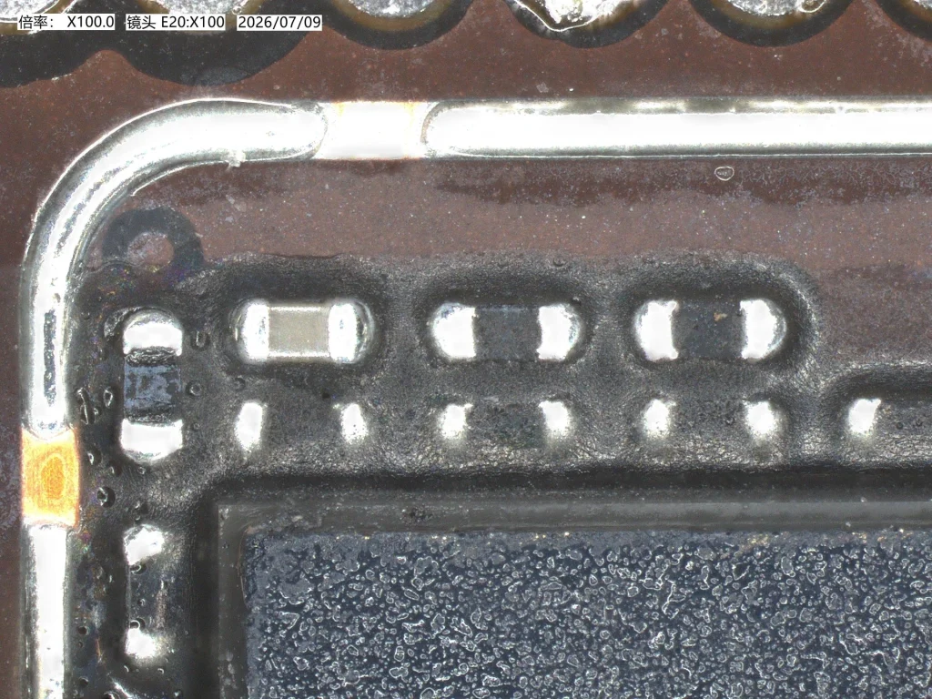
The resistors in this example contain organic surface material. MIP can remove encapsulant and adhesive residues, but it may also act on an organic protective coating once the component is exposed. The relevant control variable is therefore accumulated exposure after the component becomes visible, alongside the removal endpoint.
Controlled exposure · inspect at the endpoint
A short, staged exposure window established through DOE can balance access to resistors, pads and interconnects with surface preservation. Stop when the target is exposed and confirm electrical condition with before-and-after measurements.
Extended exposure · review the organic layer
Continued treatment after exposure can progressively thin or remove organic surface material. Coating change and failure of the resistive element require separate assessment. Pause on an abnormal appearance and review resistance, terminations and solder joints.
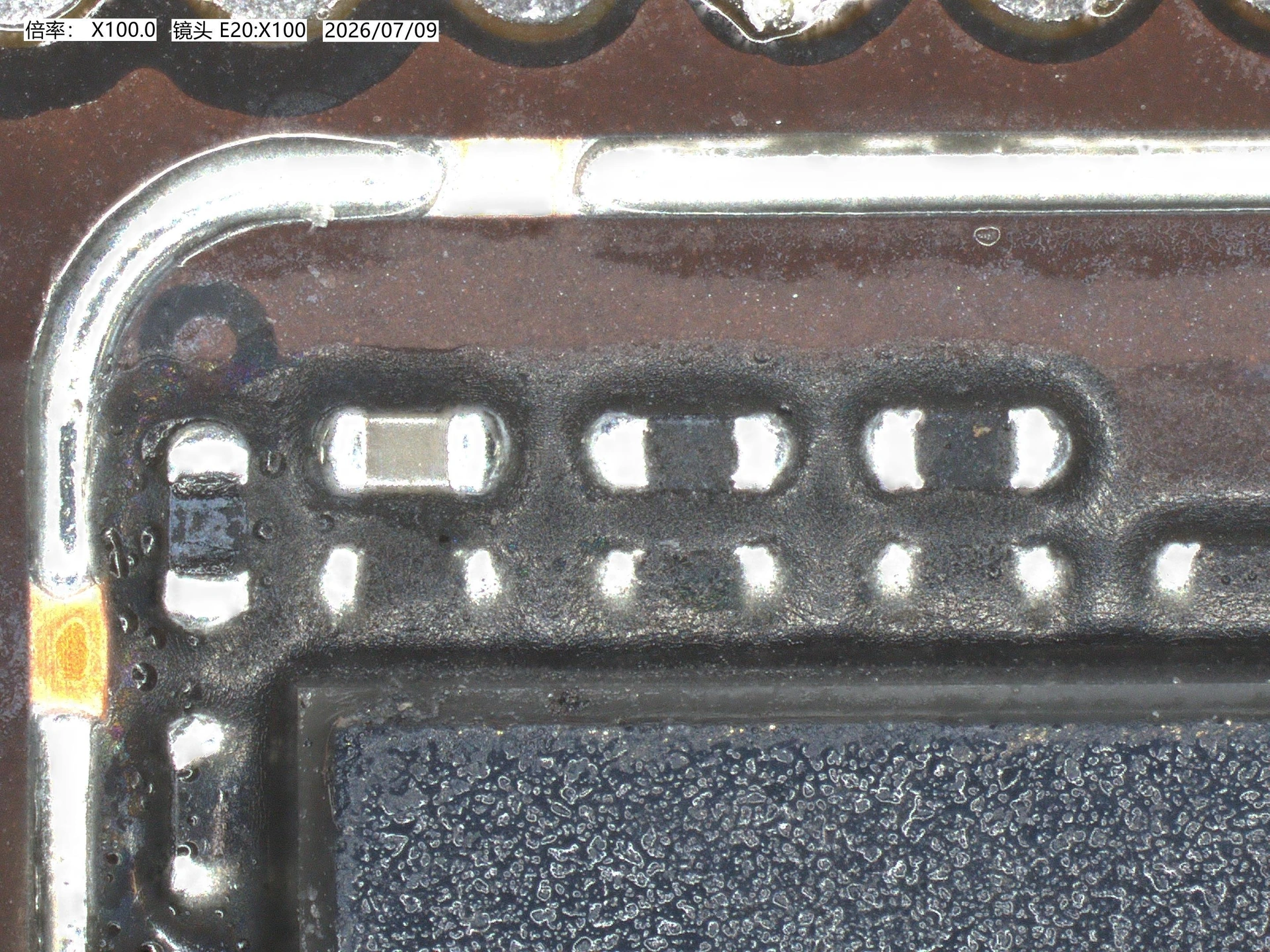
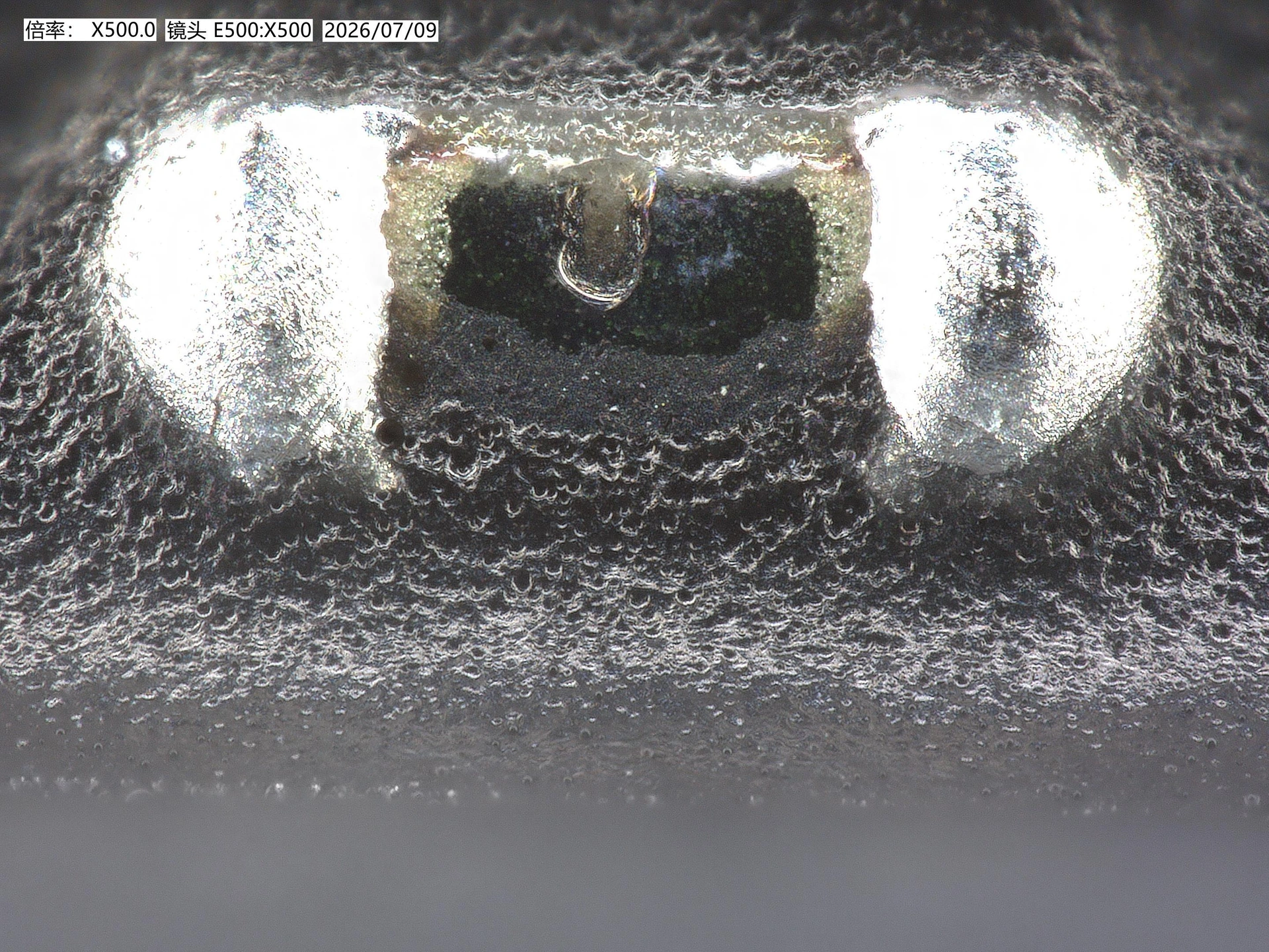
These separate board-level observations illustrate the control approach for organic-coated passives in SiP; they are not matched locations from Case A or B. Magnification and field of view differ. Appearance alone does not establish unchanged electrical performance.
DESIGN OF EXPERIMENTS
Qualify the process window
DOE (design of experiments) should identify the overlap between adequate target exposure and acceptable surface and electrical condition. Establish a recipe on representative samples, then verify its boundaries using repeat samples instead of transferring a duration from another package.
| Stage | Method | Acceptance basis |
|---|---|---|
| Baseline | Record encapsulant, filler, device identity and coating information; capture initial images and measurable electrical characteristics. | Identify organic layers, metals and interconnects to retain. |
| Experimental factors | Use supported recipe, power, temperature-management, exposure-step and cleaning-interval settings. | Define changed factors; include controls and repeat samples. |
| Staged inspection | Start conservatively and reduce inspection intervals once a component is first exposed. | Target visibility, residue, coating appearance, pads and bond structures. |
| Stop condition | Stop when the analysis objective is met; assess local protection where further processing is necessary. | Both surface and electrical acceptance; maximum cleanliness is not the endpoint. |
| Recipe validation | Record the qualified range and confirm it across representative material and device batches. | Retain process margin; requalify after material or package changes. |
Expose enough to analyze. Validate the window before reuse.
Completing exposure within a DOE-qualified short processing window, then stopping additional treatment, is central to balancing MIP adhesive removal with protection of organic layers on resistor surfaces.
SiP APPLICATION
See the complete SiP application
The same control approach is integrated into our SiP case study, alongside package structure, acid-related risks, Cases A / B and staged decapsulation. Explore SiP decapsulation and passive protection →