
Staged MIP plasma decapsulation for SiP packages integrating multiple dies, fine interconnects and passives, with DOE used to balance component exposure and protection of organic resistor coatings.
SiP structure MIP approach Cases A / B Resistor protection DOE
01 · SYSTEM IN PACKAGE
Why SiP calls for controlled decapsulation
System in Package (SiP) integrates functional dies, resistors, capacitors and other passives within one package. Substrate routing, wire bonds or flip-chip interconnects form the system. Compact dimensions bring together dense components with different heights, materials and process tolerances.
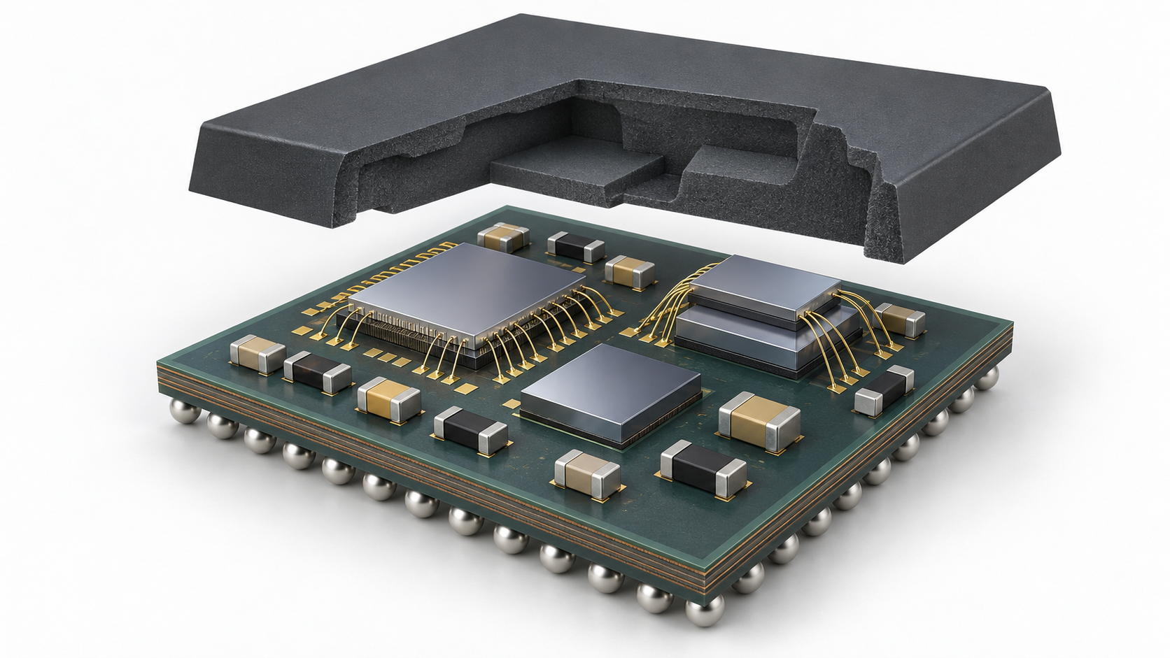
Multiple components
Dies and passives share the package, requiring access to several different regions of interest.
Different exposure stages
Taller components may emerge before deeper material is removed. Inspect endpoints by region.
Different material responses
Resin, filler, metal interconnects and organic component coatings require separate compatibility assessment.
02 · MIP DECAPSULATION
An acid-free route with a controlled endpoint
Closely spaced materials create competing requirements. Acid used to remove encapsulant can also reach thin metal pads, bond wires, terminations or existing defective interfaces. Risk depends on the metallurgy, chemistry and exposure conditions, so access must be weighed against corrosion and changes to failure evidence.
| Focus | Potential challenge with acid | MIP approach |
|---|---|---|
| Sensitive metallization | An incompatible etchant may attack pads or bond metals and affect later inspection or testing. | Use plasma species to remove organic resin without direct acid contact; verify surfaces and interconnects for the actual metal system. |
| Dense, uneven structures | Different areas reach exposure at different stages, leaving early-exposed components subject to additional treatment. | Process in stages, increase inspection frequency near exposure and evaluate local protection. |
| Residue and filler | Residue and cleaning affect visibility; wet processing also requires attention to liquid ingress and cleaning residues. | Combine organic removal with filler management using cleaning compatible with the delicate structures. |
Microwave-Induced Plasma (MIP) offers an acid-free route for sensitive packages and reduces risks associated with acid corrosion. Its value depends on suitable material selectivity and endpoint control, including protection of organic layers on exposed components.
01 Define the target
Identify dies, pads, bond regions and passives, together with the structures to preserve and the next analysis step.
02 Remove in stages
Progress with a validated recipe, compatible cleaning and intermediate images as the process approaches critical features.
03 Inspect at exposure
Use target visibility, residue and component condition to define the endpoint, then complete the required surface and electrical checks.
03 · APPLICATION CASES
Observations from two SiP packages
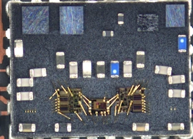
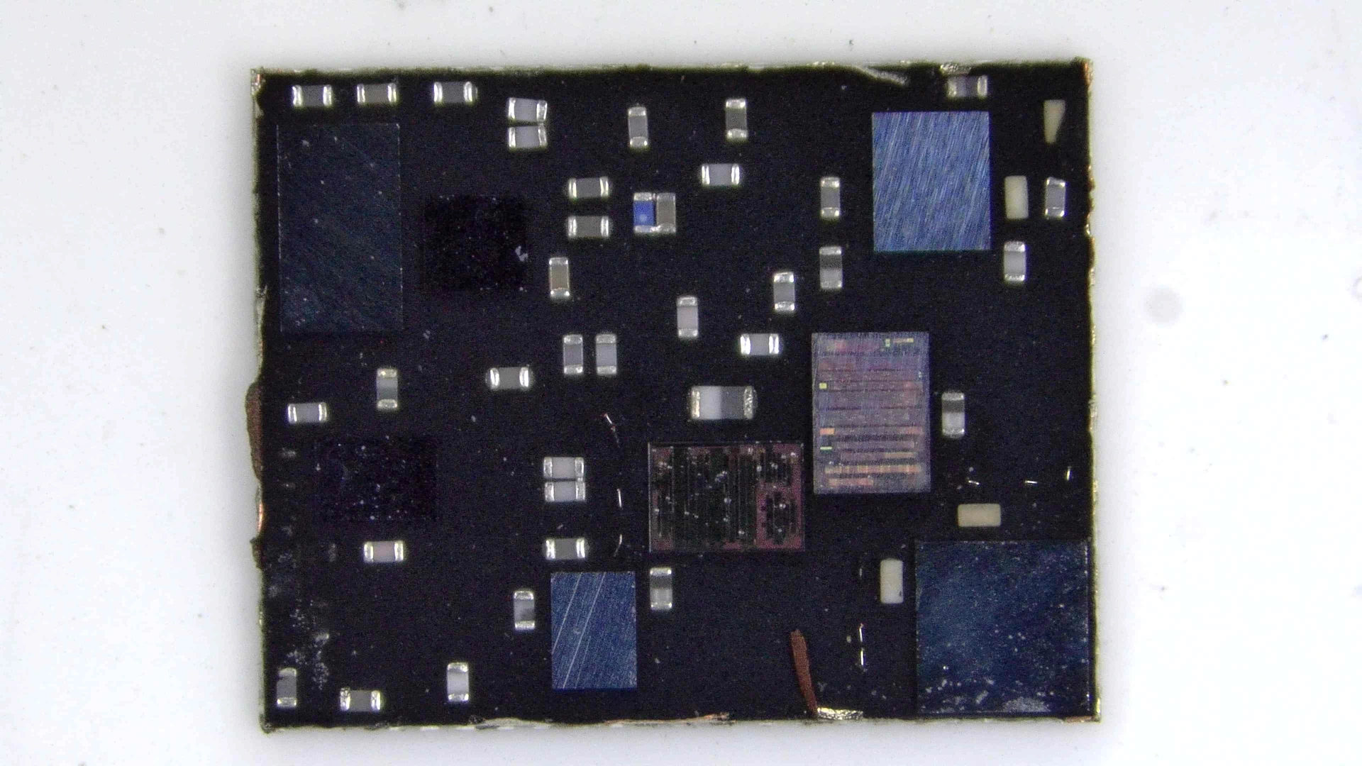
Case A · From localization to multi-die exposure
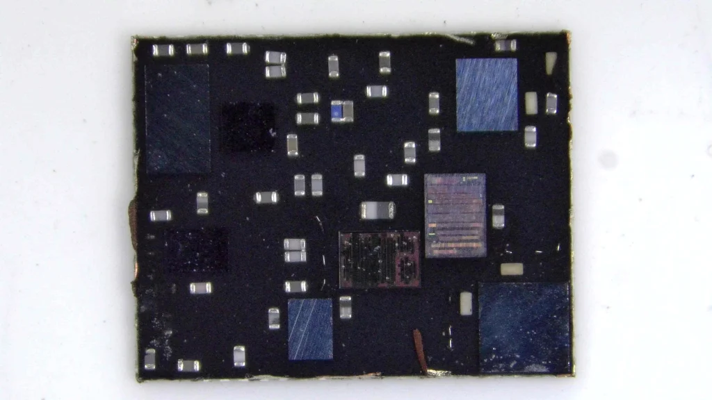
Stage images follow removal of the package material. The final view shows multiple dies and neighboring passives accessible for inspection.
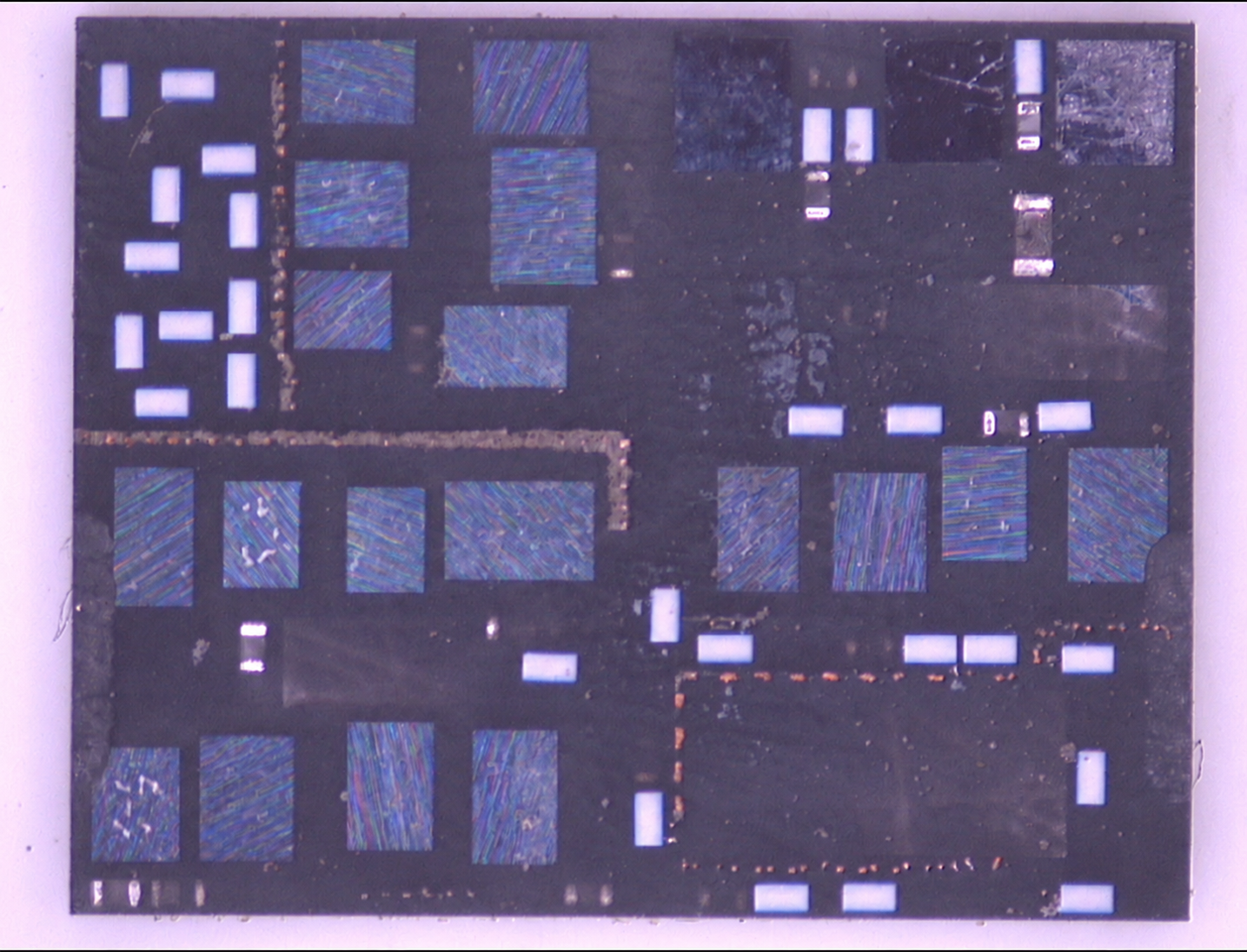
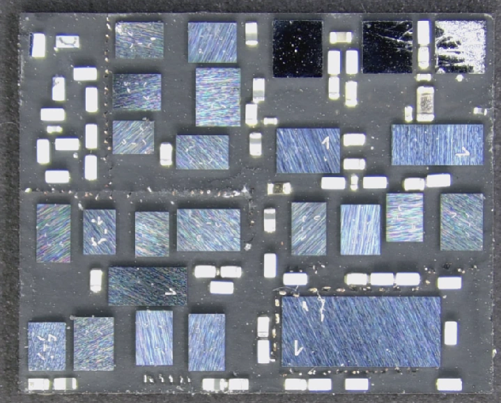
Case B · Staged access to a dense component layout
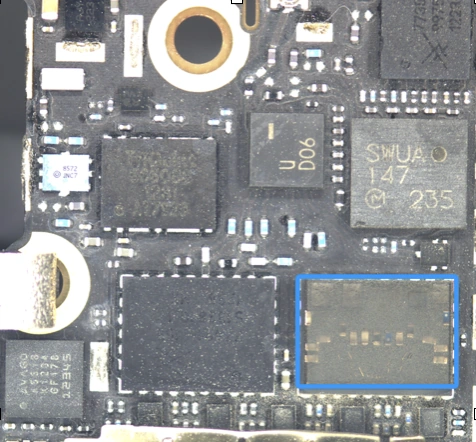
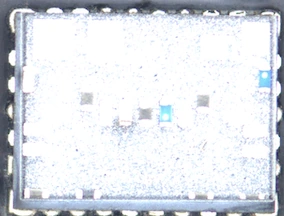
Several dies and passives occupy the same package. Residue and component exposure are reviewed region by region.
04 · PASSIVE COMPONENTS
Organic resistor coatings: control the exposure window
The resistors in this example contain organic surface material. MIP can remove encapsulant and adhesive residues, but it may also act on an organic protective coating once the component is exposed. The relevant control variable is therefore accumulated exposure after the component becomes visible, alongside the removal endpoint.
Controlled exposure · inspect at the endpoint
A short, staged exposure window established through DOE can balance access to resistors, pads and interconnects with surface preservation. Stop when the target is exposed and confirm electrical condition with before-and-after measurements.
Extended exposure · review the organic layer
Continued treatment after exposure can progressively thin or remove organic surface material. Coating change and failure of the resistive element require separate assessment. Pause on an abnormal appearance and review resistance, terminations and solder joints.
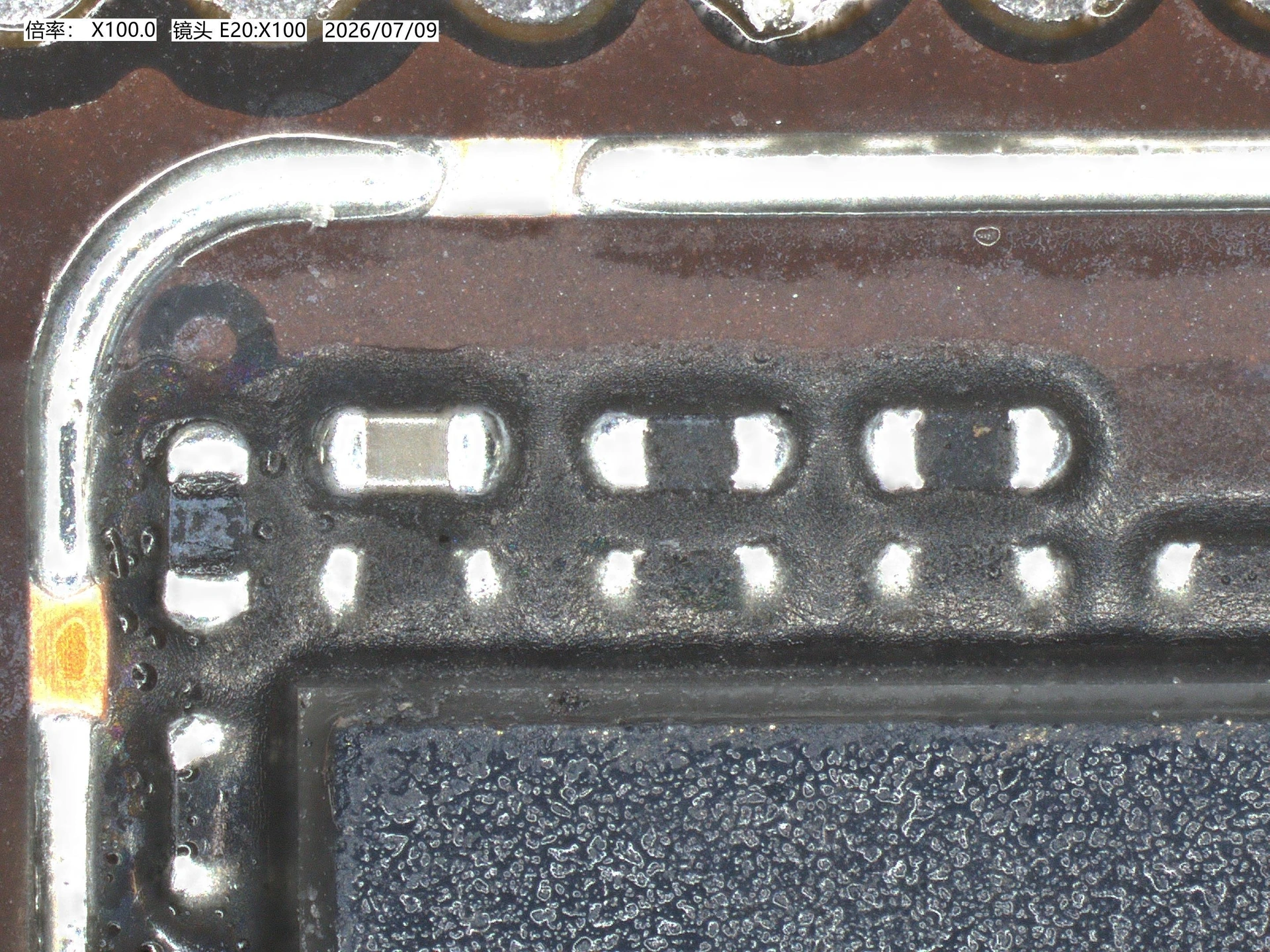
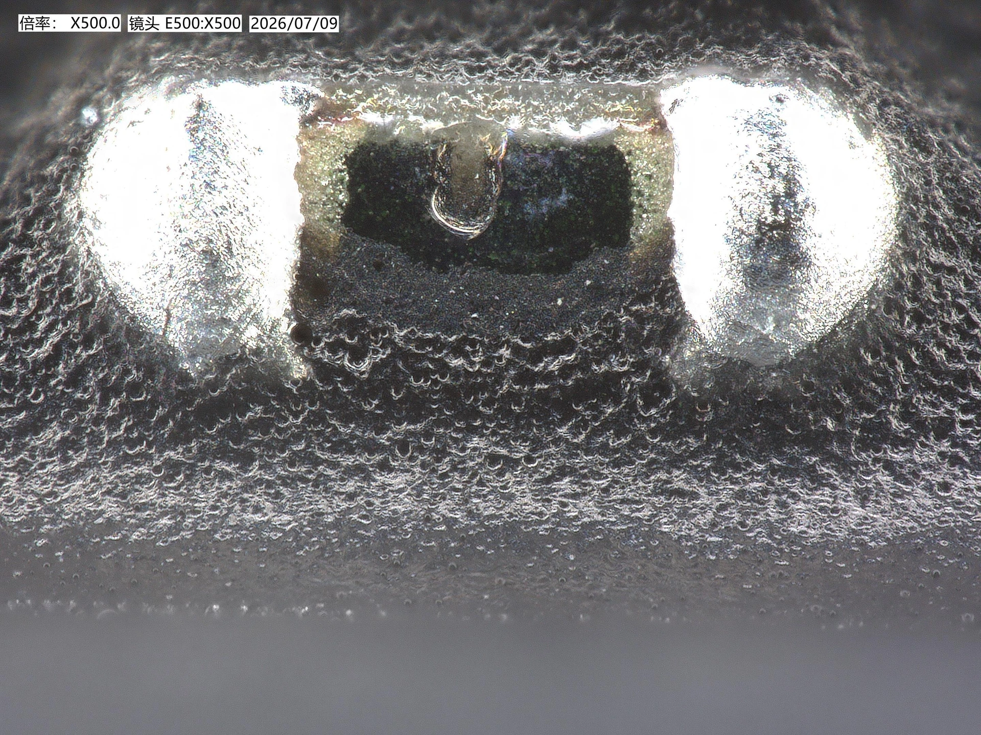
These separate board-level observations illustrate the control approach for organic-coated passives in SiP; they are not matched locations from Case A or B. Magnification and field of view differ. Appearance alone does not establish unchanged electrical performance.
05 · DESIGN OF EXPERIMENTS
Use DOE to balance removal and preservation
DOE (design of experiments) should identify the overlap between adequate target exposure and acceptable surface and electrical condition. Establish a recipe on representative samples, then verify its boundaries using repeat samples instead of transferring a duration from another package.
| Stage | Method | Acceptance basis |
|---|---|---|
| Baseline | Record encapsulant, filler, device identity and coating information; capture initial images and measurable electrical characteristics. | Identify organic layers, metals and interconnects to retain. |
| Experimental factors | Use supported recipe, power, temperature-management, exposure-step and cleaning-interval settings. | Define changed factors; include controls and repeat samples. |
| Staged inspection | Start conservatively and reduce inspection intervals once a component is first exposed. | Target visibility, residue, coating appearance, pads and bond structures. |
| Stop condition | Stop when the analysis objective is met; assess local protection where further processing is necessary. | Both surface and electrical acceptance; maximum cleanliness is not the endpoint. |
| Recipe validation | Record the qualified range and confirm it across representative material and device batches. | Retain process margin; requalify after material or package changes. |
Expose enough to analyze. Validate the window before reuse.
Completing exposure within a DOE-qualified short processing window, then stopping additional treatment, is central to balancing MIP adhesive removal with protection of organic layers on resistor surfaces.
06 · QUESTIONS & ANSWERS
SiP MIP decapsulation questions
Why evaluate MIP for SiP decapsulation?
SiP combines multiple dies and passive components. MIP provides an acid-free resin-removal route that can reduce acid-corrosion risks, with staged processing and inspection used to control exposure of sensitive features.
Can MIP remove organic material on a resistor?
Yes. In this example, the resistor surface includes an organic layer that can thin or be removed with excessive accumulated exposure. A DOE-qualified short exposure window, a timely stop and appropriate local protection help manage that risk.
How is the endpoint determined?
First confirm that the target is sufficiently exposed for the analysis objective. Then review residue, protective coatings, terminations and interconnects. Where function must be retained, verify resistance or relevant electrical properties using agreed methods.
Can a recipe be transferred directly to another package?
It requires confirmation. Changes in resin, filler, coatings or component height can change the exposure sequence and acceptable window. Revalidate on representative samples.
07 · NEXT STEP
Define a testable process for your SiP sample
System in Package (SiP)
An integration approach combining multiple dies, passive components and interconnects in one package.
MIP plasma decapsulation
Removal of organic encapsulation material using species generated by microwave-induced plasma.
DOE process window
A parameter range experimentally qualified to meet both exposure and component-preservation requirements.
Explore MIP equipment Explore iPlasma Pro Discuss sample evaluation and DOE →