
Sample and analysis objective
Board-level adhesive removal must distinguish encapsulant and solder mask from solder and copper structures that must remain. Different materials and objectives require separate endpoint criteria.
| Item | Case information |
|---|---|
| Removal targets | Encap adhesive and PCB solder mask |
| Sample level | Local board-level region |
| Acceptance basis | Agreed exposure area, surface condition and electrical requirements |
Processing record
The source uses two local board images to illustrate Encap adhesive and PCB solder-mask removal, without a common processing time or residual-thickness measurements.
Actual sample images
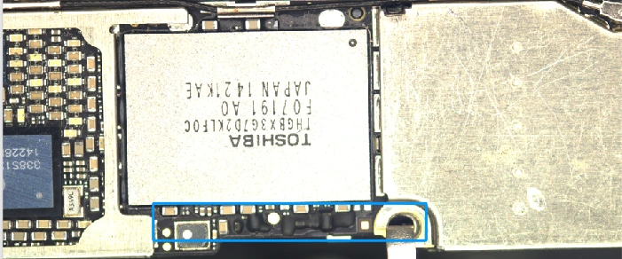
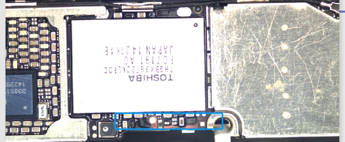
Result review priorities
- Define which metals may be exposed and which structures must remain.
- Do not equate adhesive removal alone with readiness for resoldering.
- For rework, separately inspect original solder thickness, pad condition and resolderability.