
APPLICATION OVERVIEW
Reveal the connections. Across the stack.
Stacked-die decapsulation must expose internal connections while preserving access to bond wires, pads and die edges. Microwave-induced plasma (MIP) supports controlled removal of organic encapsulation material. Treating different sides in stages, with inspection between steps, helps reveal connections at depth. For memory packages containing stacked dies, inspection can extend to a selected layer through a separate delayering workflow. Two examples illustrate stack exposure and staged plasma removal, followed by a conceptual route combining iMech Pro grinding with MIP residue removal.
Stacked dies
Expose die edges and access to deeper regions.
Multi-tier wires
Review wire loops, bonds and residue beneath them.
Two real samples
Stack exposure and staged plasma-only processing.
CHALLENGES / MULTILAYER & MEMORY PACKAGES
Removing the cover is only the beginning.
Access at depth
Multiple dies, dense wire loops and sidewalls obstruct one another. Lower pads, under-wire residue and a target die may remain hidden after the top is exposed. The target layer determines the next analysis steps in a stacked memory package.
Sensitive interconnects
Fine wires and thin pad metallization are sensitive to processing. Incompatible acid chemistry can introduce corrosion, while pulling or contact can disturb wire loops. Preparation should minimize new damage that could obscure the original failure.
Residue and fillers
Molding compound, die-attach film (DAF), and film-over-wire (FOW) material in some architectures can cover inspection regions. Organic residue may still obscure the next die and its connections after the upper silicon has been removed.
THE MIP APPROACH
Expose the connections. Then access the target layer.
Controlled organic-material removal
MIP reactive species act on accessible organic material to reveal die edges, wires and pads progressively. Conditions are matched to metals and resins, offering a dry-process route to evaluate for acid-sensitive structures.
Staged access and inspection
Adjust orientation, process in stages and inspect multiple focal planes to address occlusion and deeper under-wire regions. Judge the endpoint by access to the target structure, not just a visible top surface.
Connect delayering with residue removal
For lower-die access, control silicon removal and organic-residue removal separately: iMech Pro provides controlled grinding, followed by MIP treatment of accessible adhesive to establish the next inspection window.
Metallization, adhesive chemistry and fillers vary between packages, so representative samples establish the process conditions. The two examples show stacked-die exposure and staged removal.
CASE 01 / STACK EXPOSURE
From the die stack to individual connections.
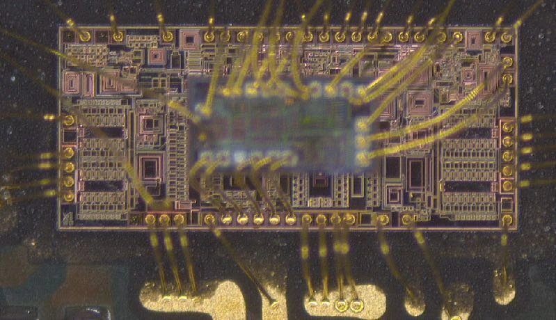
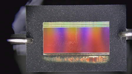
Case 01 shows the overall layout and local structures after opening a stacked-die package. Oblique views and different focal planes help distinguish die edges, wire-loop heights and bond positions, supporting target-die identification and further analysis.
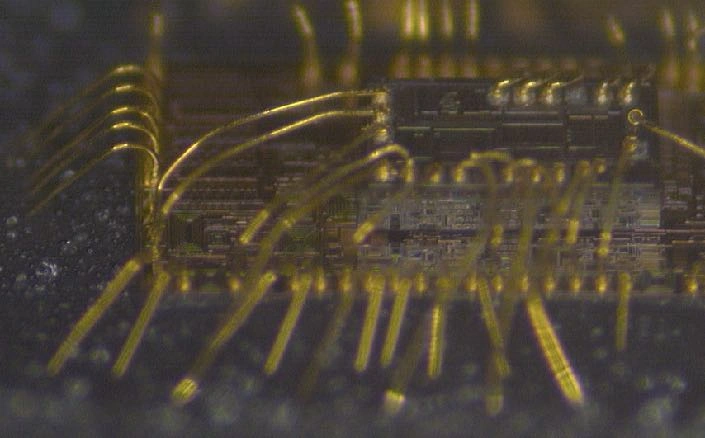
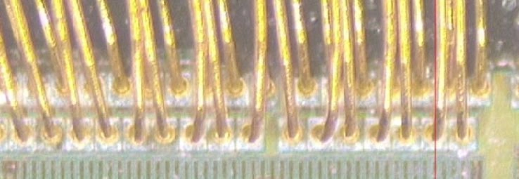
These images document the exposed structure and appearance. Processing time and electrical retest results are not specified for this sample.
CASE 02 / STAGED PLASMA REMOVAL
Plasma only. Deeper access, side by side.
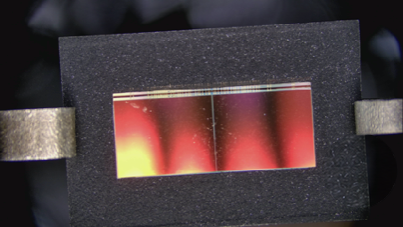
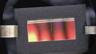
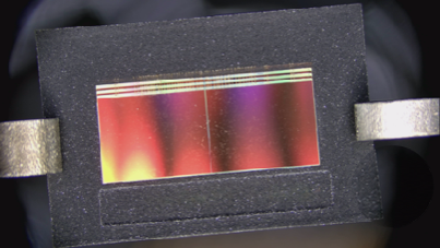
Case 02 was processed using plasma only, with no laser pre-opening. The record shows four bond-wire tiers exposed on one side after approximately 2 hours; the deeper region on the other side has a recorded processing time of approximately 3 hours. Four tiers refers to the wires. These are separate side-specific records, not a universal total cycle time.
Side A · Four-stage progression
The four photographs follow the recorded sequence. The Side A treatment record is approximately 2 hours; individual frame times were not recorded.
Side B · Approx. 3-hour record
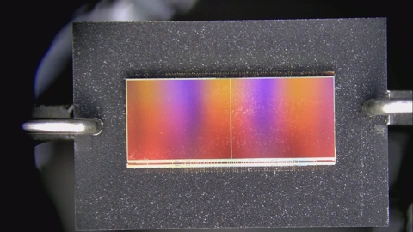
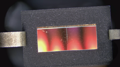
Stage images document removal progress and retain the resolution limits of the originals. Views and magnification are not calibrated for dimensional comparison.
Inspection focus: loops, bonds and the space beneath
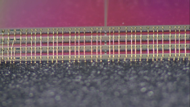
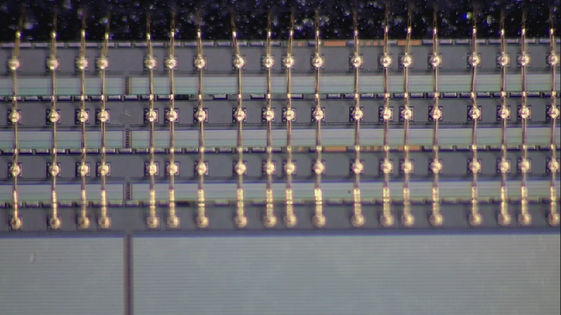
Photographs retain the original field of view and orientation; only edge microscope controls have been removed. The microscopy video shows a local moving view. Wires, visible defects and residue have not been retouched.
NEXT STEP / DIE DELAYERING
From an opened stack to the next die.
When the target lies beneath an upper die, a combined iMech Pro and MIP route can be evaluated after decapsulation and localization. Controlled mechanical grinding removes selected upper silicon; MIP then treats accessible organic interlayer residue to create the next inspection window. The render below explains this workflow; it does not document follow-on tests on the two samples above.
Mechanical delayering + MIP residue removal
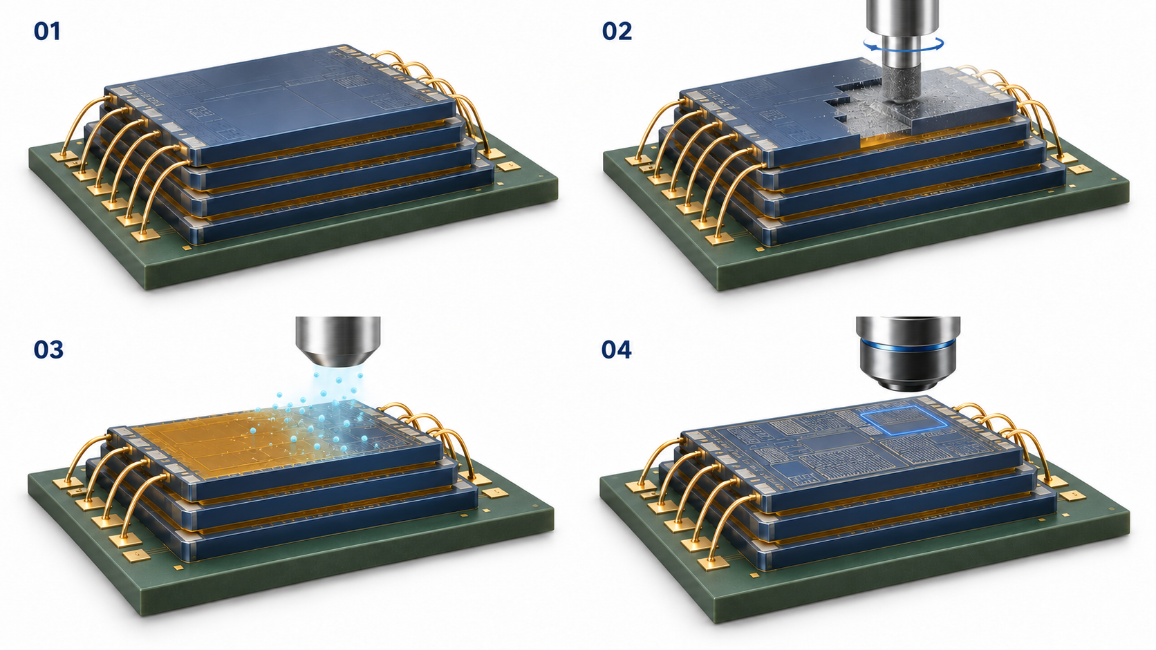
01 · Expose and locate
Remove external encapsulation, identify the target layer and connections to retain, and document existing defects and microscopic features.
02 · Controlled iMech Pro grinding
Grind in stages according to target depth and remaining thickness, approaching the interface progressively. Assess wires belonging to the upper die and protect or manage them according to the analysis plan.
03 · MIP interlayer-residue removal
Treat accessible organic residue exposed by mechanical removal. Assess conditions for the actual DAF or FOW formulation and inspect fillers, lower pads and bond wires.
04 · Inspect the next die
Inspect the newly accessible die and proceed with failure analysis. For a deeper target, reassess the next interface before repeating delayering and residue removal.
Blue-gray represents silicon dies, amber the interlayer adhesive, and gold the bond wires. Stage 01 illustrates four dies; after removing the uppermost die, stages 03–04 show the remaining three.
Delayering consumes the selected upper die, so complete any required inspection or testing of that layer first. The MIP step shown treats organic residue and does not replace silicon grinding. Closed interfaces require an access path. Validate the area, endpoint and structures to retain on representative samples.
iPlasma MIP
For stacked-package decapsulation and treatment of accessible organic residue after mechanical delayering.
iMech Pro
For evaluating controlled grinding and access to selected layers, followed by MIP residue removal.
RESULT REVIEW
Visibility enables the next analysis step.
| Inspection region | What to examine |
|---|---|
| Bond-wire tiers | Examine loops, crossings, occlusion, and visible breaks or contact between wires at each tier. |
| Bonds and pads | Review bond positions, pad surfaces and surrounding material, increasing magnification where needed. |
| Die edges and under-wire regions | Inspect deep residue and fillers; decide whether more treatment is needed for the intended analysis. |
| Electrical function | Retest independently when function or data must be preserved; optical appearance does not establish electrical integrity. |
COMMON QUESTIONS
About stacked-die plasma decapsulation
Why inspect different sides of a stacked-die package?
Dies, wire tiers and sidewalls obstruct one another. Multiple sides and focal planes help reveal deeper residue and bond regions, rather than judging the endpoint from a top view alone.
Can MIP expose a package while preserving its bond wires?
The images show multi-tier wires observable after decapsulation. The process must be matched to wire and pad metals, encapsulation materials and temperature requirements. Wire appearance and electrical continuity should be checked separately.
Can the 2- and 3-hour records be used as standard cycle times?
These values apply only to the different sides of the sample in Case 02. Package dimensions, resin, fillers, access and the required endpoint affect processing time. Representative samples are needed for a throughput estimate.
What does memory-chip delayering mean here?
This page concerns multiple dies stacked within a package: removing a selected upper die and interlayer material to access a lower target die. It is different from analyzing the internal cell layers of a single 3D NAND die.
Stacked-die decapsulation
Removal of package material to inspect vertically stacked dies and interconnects for semiconductor failure analysis and structural examination.
Microwave-induced plasma decapsulation
Use of reactive species generated by microwave-induced plasma to remove accessible organic encapsulation material, with conditions matched to the materials and target structure.
Package-level memory-die delayering
Sequential removal of overlying silicon and interlayer material in a stacked memory package to create access for structural inspection and failure analysis.