MIP · MICROWAVE-INDUCED PLASMA
What is microwave-induced plasma (MIP)?
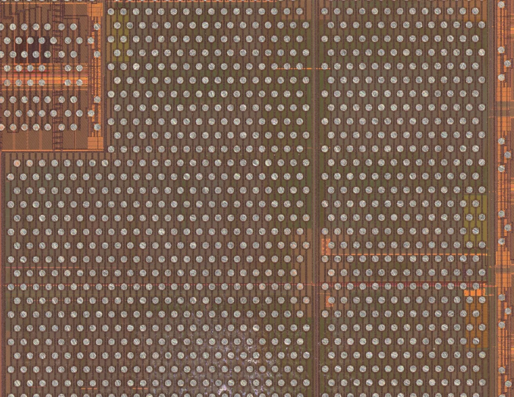
MIP stands for Microwave-Induced Plasma. In chip decapsulation, microwave energy excites a process gas to generate reactive species, primarily oxygen radicals, that react with organic encapsulation resin. Gradual removal exposes the die, bond wires, pads and interconnect regions.
ICDECAP uses an argon/oxygen process route focused on selective organic-resin removal. Inorganic fillers such as silica may require a separate cleaning step after the resin recedes. Organic materials, fillers and metals respond differently, so their endpoints must be assessed separately.
01
Microwave excitation
Microwave energy excites the process gas to produce reactive species for resin removal.
02
Organic-material reaction
Reactive oxygen attacks the organic matrix, progressively creating access to the target structure.
03
Exposure and inspection
Inspect residue, fillers and critical surfaces between stages, then proceed to microscopy, SEM–EDS or electrical analysis.
What is atmospheric-pressure MIP?
Atmospheric-pressure MIP uses microwave-induced plasma to remove organic encapsulation materials near ambient atmospheric pressure. No vacuum environment is required for decapsulation, simplifying sample loading, staged inspection and integration with other preparation steps.
01
No vacuum cycle
Processing takes place at atmospheric pressure, without the pump-down and venting cycle required by a vacuum chamber.
02
Designed for staged processing
Inspect the exposed structures between processing stages, then continue removal as needed. MIP can follow laser preprocessing or local opening with iMech Pro.
What are the benefits of MIP decapsulation?
MIP offers a controllable resin-removal route that reduces acid exposure and direct mechanical contact, progressively exposes delicate structures and aims to retain useful failure evidence. Selectivity depends on matching the recipe to the materials and validating it on representative samples.
01
Reduce acid-corrosion risk
An acid-free removal route for thin aluminium pads, copper and palladium-coated copper wires, and solder interconnects helps reduce changes caused by aggressive acid chemistry.
02
Approach delicate structures
Reactive-species processing reduces the need to keep scraping or grinding mechanically near fine wires, pads and sensitive surfaces.
03
Retain useful evidence
Progressively reveal metal filaments, bridging and adjacent voids so location, morphology and composition can be assessed together.
04
Support follow-on analysis
Where required structures and electrical paths remain intact, proceed to optical microscopy, SEM–EDS, bond inspection and pre-/post-opening electrical comparisons.
Which decapsulation problems can MIP address?
MIP is useful when the goal is to expose fine metal features, thin pads, buried interconnects or foreign matter that may be affected by acid chemistry or continued mechanical removal. It provides a finishing step tailored to the materials and analysis objective.
| Application / target | Preparation challenge | MIP approach |
|---|---|---|
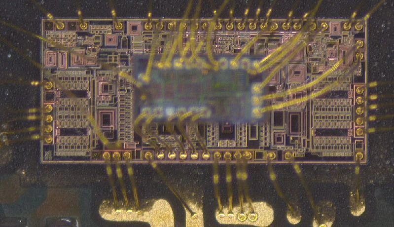
| Small MEMS / thin aluminium pads | Acid may attack thin aluminium, changing the pad surface or causing pad loss. | Remove the covering resin without acid and inspect pads between stages.Explore the MEMS case ↗ |
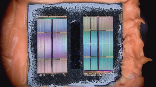
| Stacked die / memory packages | Resin surrounds fine wires at multiple levels, complicating access without disturbing the interconnect structure. | Expose wire loops and pads in stages, then plan layer-by-layer analysis as needed.Explore stacked-die decapsulation ↗ |
| SiP / embedded passive components | Different dies, solder materials and organic resistor coatings coexist in one package. | Use DOE to establish a short exposure window and inspect as soon as components become visible.Explore the SiP case ↗ |
| Flip chip / micro-shorts | Residual resin obscures fine metallic foreign matter; acid cleaning or contact may disturb fragile connections. | Expose metal filaments and adjacent voids through organic removal before morphology and composition analysis.Explore the micro-short case ↗ |
| 3D packages / Underfill | Resin remains after precision grinding; further grinding or acid treatment may disturb micro-interconnects. | Create targeted access with iMech Pro, then use MIP for local residue removal.Explore the 3D-package case ↗ |
Stop at sufficient exposure. MIP can also remove organic protective layers that need to remain and may modify some material surfaces. Include gas recipe, power, temperature, exposure time and filler cleaning in DOE. Inspect at exposure and verify electrical preservation through measurement.
With iPlasma: add MIP to your existing preparation flow
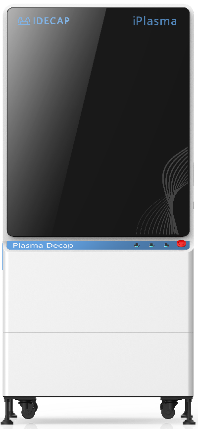
iPlasma provides standalone MIP processing. Thick molded packages are typically pre-opened with an external laser. For local buried targets, iMech Pro can establish access before MIP removes organic residue around the target region.
External laser or iMech Pro preparation iPlasma MIP Inspection and analysis
For fine decapsulation, removal of residual material after preprocessing and staged observation of critical regions.
Focus on critical areas
Adjust the processing region around the observation target, preserving structural information for subsequent microscopy.
Connect with prior preparation
Apply fine processing after laser opening to build a staged preparation workflow.
Assess material response
Evaluate removal and process effects for encapsulants, fillers and metal systems.
Technical overview
| Item | Published specification / application information |
|---|---|
| Core process | Atmospheric-pressure MIP plasma |
| Primary objective | Removal of organic encapsulation and residual material |
| Observation targets | Die surfaces, bond wires, pads and related structures |
| Supporting workflow | Opening, finishing, cleaning and microscopic review |
Adhesives, inorganic fillers, sensitive surfaces and metal combinations respond differently. Validate the process window using representative samples.
Suggested process sequence
- Confirm the structure
- Finish selected areas
- Inspect the surface
Information for sample evaluation
- Package and material type, target structures and areas to preserve
- Sample dimensions, structural images, failure state and downstream analysis method
- Agreed methods for surface, structure or thickness verification
Validate the plasma process window around the target structure
The MIP technical material emphasizes an internal-electrode-free source, high plasma density and control of particle bombardment. Application evaluation must still check organic removal, filler residue and metal surfaces, particularly thin aluminum and deep bond structures.
MIP principles and validation priorities → Plasma-only decapsulation records →
MIP · 2025 · MULTI-TORCH & LARGE-FORMAT
Independent settings. Batch decapsulation. More sample flexibility.
Introduced in 2025, iMech Duo, Trio and Quad feature individually configurable atmospheric-pressure MIP torches. Compare parameter sets in parallel for rapid process validation, then load multiple samples at each station for batch decapsulation. iMech Plus supports both localized opening of chips mounted on large PCBAs and loading multiple individual samples for batch processing.
Scroll horizontally to compare all four configurations →
| Configuration | iMech DuoDual torch | iMech TrioTriple torch | iMech QuadQuad torch | iMech PlusLarge format · multiple samples |
|---|---|---|---|---|
| Equipment appearance | 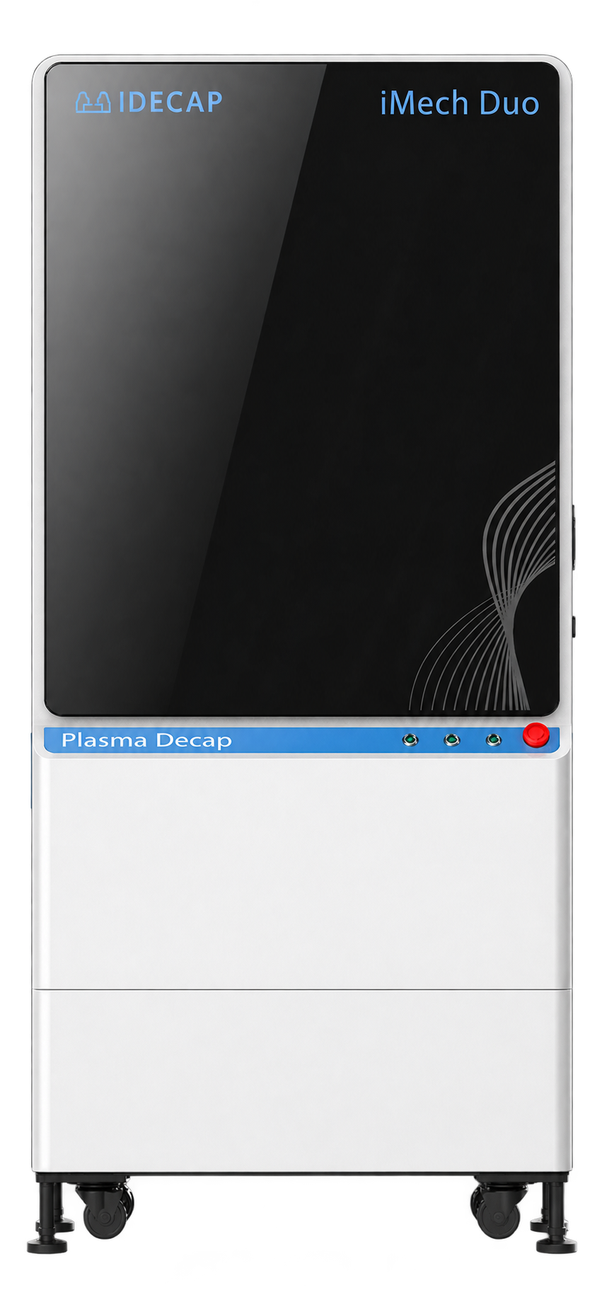 Model exterior reference | 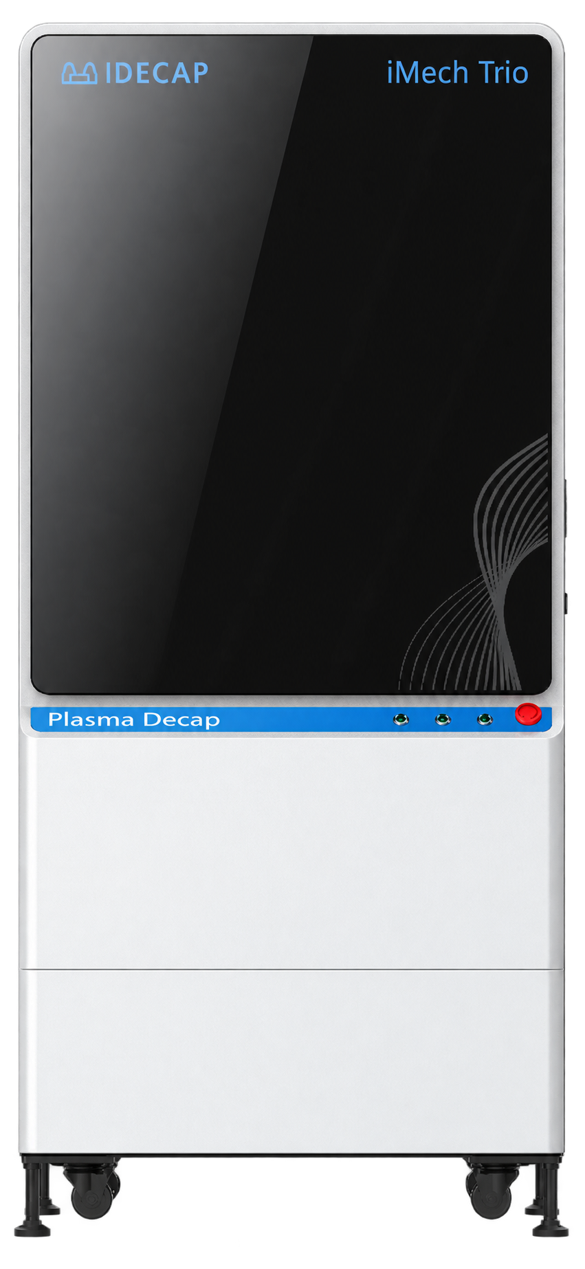 Model exterior reference | 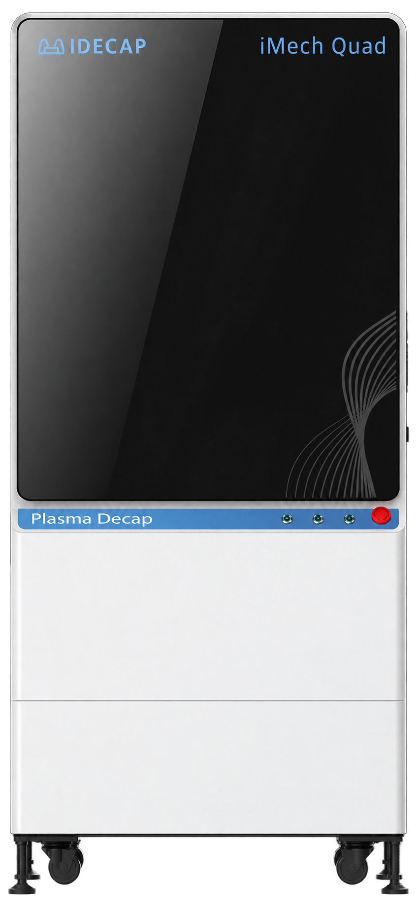 Model exterior reference | 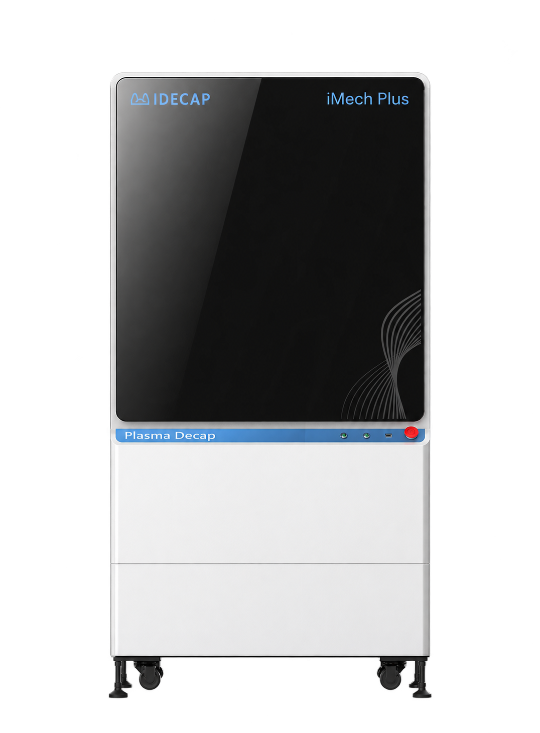 Model exterior reference |
| Application layout | 2 independent torches · multi-sample batches | 3 independent torches · multi-sample batches | 4 independent torches · multi-sample batches | On-board chips / individual sample batches |
| Core benefit | Dual-torch process validation and batch decapsulation | Triple-torch process validation and batch decapsulation | Quad-torch process validation and batch decapsulation | Large-PCBA on-board opening and multi-sample batches |
| Application fit | Set parameters separately for two torches to compare process conditions. Load multiple samples in a single lane at each station, moving from validation into batch decapsulation. | Set parameters separately for three torches for rapid comparison and validation. Load grouped samples for repeated preparation tasks and batch decapsulation. | Set parameters separately for four torches for parallel process validation. Closely spaced sample lanes at each station support efficient batch decapsulation. | Accommodate a large PCBA and fixture for localized opening of a mounted chip, or load multiple individual samples together for batch processing. Define layout and protection around board size, chip dimensions and adjacent components. |
Sample quantities in the drawings are illustrative, not a fixed or maximum capacity. Actual loading and spacing depend on chip dimensions, fixtures and process layout; throughput depends on materials, opening area and recipe. Enclosures and application layouts are illustrative. Plus on-board processing also requires the working area and protection to be defined around component heights and target location.
Share your sample volume and target cycle time, or PCBA dimensions and target-chip location, to discuss the appropriate MIP configuration with ICDECAP.