
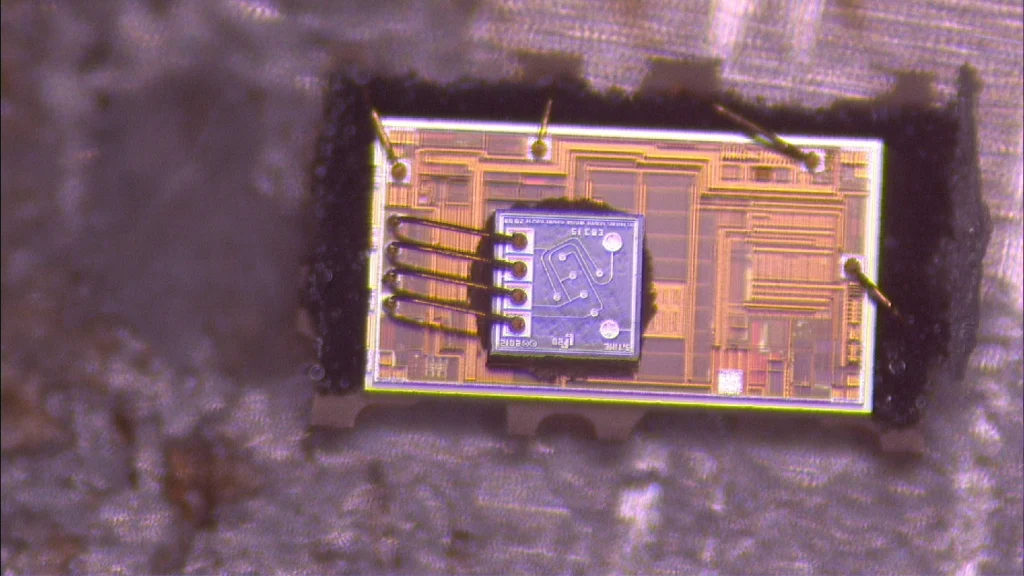
A small MEMS device. A thin aluminum layer worth preserving.
This application concerns small MEMS (microelectromechanical systems) devices with a very thin aluminum layer on their pads. Preparation must remove surrounding encapsulation while preserving the sensitive pad metallization and its bond connections. Pad integrity is therefore a key measure of decapsulation quality.
IDECAP uses MIP (microwave-induced plasma) to combine organic encapsulant removal with thin aluminum pad protection, reducing corrosion risk associated with direct exposure of sensitive aluminum to decapsulation acids.
The challenge: exposing the device without losing the pad.
For these thin-pad samples, conventional acid decapsulation can attack aluminum while removing the encapsulant. With little margin for metal loss, localized corrosion may result in missing pad metal, pad detachment or damage around a bond connection. Risk depends on acid chemistry, temperature, exposure time and sample structure.
Preparation-induced corrosion or pad loss can complicate failure analysis. The pad and connection being investigated may already have changed, making it harder to distinguish the original failure from an artifact of decapsulation.
The MIP approach: remove encapsulant and preserve the connection.
MIP can use oxygen-related reactive species to remove the organic matrix of encapsulation materials, providing an acid-free route around thin aluminum pads. For these samples, IDECAP focuses on exposing the target area while preserving pads, bond sites and surrounding structures for microscopy and failure analysis.
| Preparation challenge | IDECAP MIP focus |
|---|---|
| Acid-sensitive thin aluminum | Avoid direct contact between the pad and decapsulation acids; match plasma conditions to the material system. |
| Pad loss or connection damage | Use staged treatment and inspection near the target area, focusing on pad edges, metal continuity and bond sites. |
| Sensitive structures in small MEMS | Assess exposure time, temperature rise and particle-cleaning methods to suit the device and target region. |
A preparation workflow built around pad protection.
01 · Define the sample and preservation targets
Identify the MEMS package structure, pad locations, available aluminum-layer information and analysis objectives. Record accessible images and electrical condition before preparation.
02 · Plan controlled material removal
Select any necessary pre-removal method and opening area for the package. Retain a suitable processing margin when approaching thin aluminum pads and sensitive regions.
03 · Apply staged MIP finishing
Progressively remove remaining organic encapsulant. Inspect as pads and bond sites become exposed and avoid unnecessary continued exposure. Select a compatible method for residual fillers or particles.
04 · Review pads and bond connections
Inspect metal surfaces, pad edges, connection sites and visible residue. Add thickness, cross-section or electrical measurements as required by the analysis.
Actual micrograph: inspect the pads and bond regions.
The original micrograph above shows the small central die and surrounding bond connections. Inspection should focus on pad surfaces and edges, structures around the bond sites, and any visible corrosion, missing metal, detachment or obscuring residue.
This application illustrates the value of MIP for small MEMS preparation, thin aluminum bond-pad protection and acid-sensitive device decapsulation. The image documents the regions shown; retained metal thickness and electrical performance require corresponding measurements.
Frequently asked questions
Why should standard acid-decapsulation conditions not be assumed suitable for thin-pad MEMS?
The aluminum pad layer in these devices is very thin. Incompatible acid chemistry or exposure conditions may attack the metal and introduce pad loss, detachment or connection defects. The process should be qualified specifically for pad preservation.
How does MIP help protect thin aluminum pads?
MIP provides an acid-free route for removing organic encapsulation, limiting direct pad exposure to decapsulation acids. Staged processing and inspection support preservation of sensitive regions. Conditions must still match the encapsulant, pad metallurgy and MEMS structure.
Define a decapsulation route for your MEMS sample.
Share package images, pad metallurgy, structures to preserve and analysis objectives. IDECAP can evaluate a MIP preparation route and review criteria centered on thin aluminum pad protection.
Explore iPlasma MIP → Discuss your MEMS sample →
Process evaluation should account for the encapsulant, pad metallurgy and MEMS structure. Aluminum-layer preservation and electrical performance require appropriate measurements.